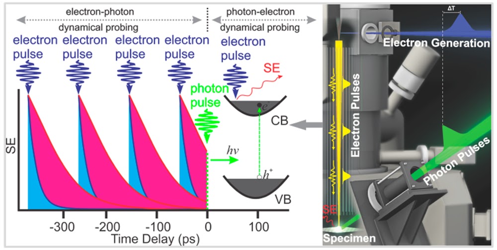
Imaging of Carrier Dynamics by Second-Generation 4D Scanning UEM enabled by Model IMPULSE from Clark-MXR. A new publication from Prof. Omar Abdelsaboor group at KAUST
Jingya Sun, Vasily A. Melnikov, Jafar I. Khan, and Omar F. Mohammed
Solar and Photovoltaics Engineering Research Center, Division of Physical Sciences and Engineering, King Abdullah University of Science and Technology (KAUST), Thuwal 23955-6900, Kingdom of Saudi Arabia

Abstract
In the fields of photocatalysis and photovoltaics, ultrafast dynamical processes, including carrier trapping and recombination on material surfaces, are among the key factors that determine the overall energy conversion efficiency. A precise knowledge of these dynamical events on the nanometer (nm) and femtosecond (fs) scales was not accessible until recently. The only way to access such fundamental processes fully is to map the surface dynamics selectively in real space and time. In this study, we establish a second generation of four-dimensional scanning ultrafast electron microscopy (4D S-UEM) and demonstrate the ability to record time-resolved images (snapshots) of material surfaces with 650 fs and ∼5 nm temporal and spatial resolutions, respectively. In this method, the surface of a specimen is excited by a clocking optical pulse and imaged using a pulsed primary electron beam as a probe pulse, generating secondary electrons (SEs), which are emitted from the surface of the specimen in a manner that is sensitive to the local electron/hole density. This method provides direct and controllable information regarding surface dynamics. We clearly demonstrate how the surface morphology, grains, defects, and nanostructured features can significantly impact the overall dynamical processes on the surface of photoactive-materials. In addition, the ability to access two regimes of dynamical probing in a single experiment and the energy loss of SEs in semiconductor-nanoscale materials will also be discussed.

