About Milt Vardakis

This author has not yet filled in any details.
So far Milt Vardakis has created 5 blog entries.

Increasing Speed to Market With Innovative Products and Services

Companies with streamlined product development capabilities gain improved competitive advantages with increased ability to predict time-to-market, and allocation of resources for rolling out the product at the right time and place.  Speed to Market product timelines contain four milestone periods: 1) generation of the product idea; 2) complete design cycle; 3) development; and, 4) market launch. Skilled execution of these four stages, coupled with closely managed supply chain resources, ensures that business plans are optimized, and investors' expectations are fulfilled. Effective supply chains demand alliances with partner organizations who can offer uniquely innovative products and services that quickly adapt to changing market trends and are [...]

2019-07-31T23:17:54+00:00Jul 31, 2019|

Smarter Internet Of Things Becomes Intelligence of Manufacturing Things

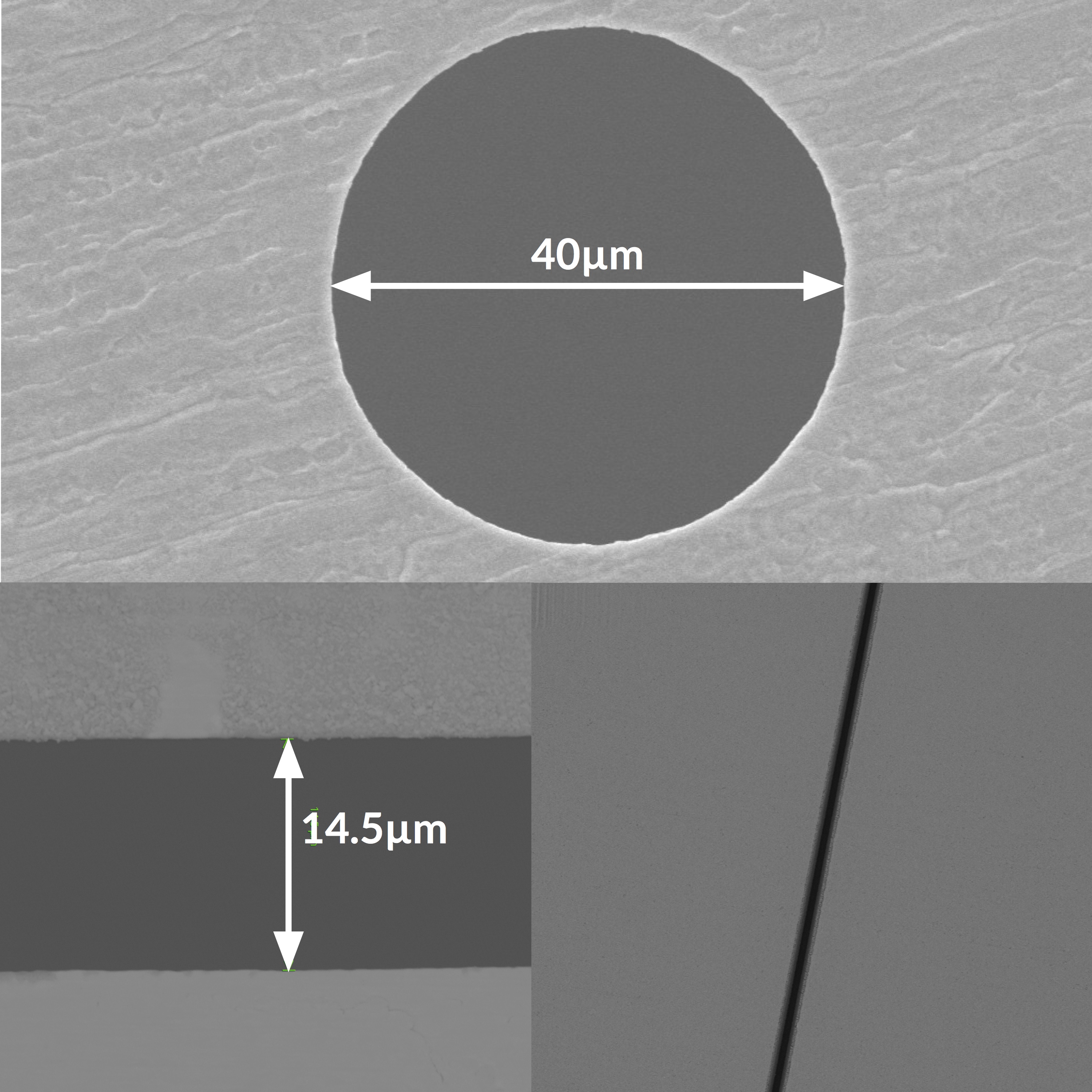
2019 marks a definitive milestone for IoT, largely influenced by the upcoming launch of 5G in 2020. We already know that everything that can be connected will be connected. The next step is to build microscopic IoT gadgets whose design trends require niche-integrated, multifunctional solutions in the shape of different sensors that include connectivity. Mechanical and electrical engineering design trends towards monolithic componentry will be enabled by optimized mechanical and laser micromachining processes that support sensor applications in wireless communications, smart clothes, smart watches, Fitbits and automobiles. Consequently, demands for smaller microholes, on tighter [...]

2019-04-26T18:53:18+00:00Apr 24, 2019|

Femtosecond Laser Micromilling Application Examples: Serial Sectioning and Wear-Defect Simulation

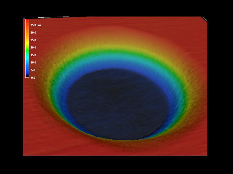
Femtosecond laser micromilling, or ablative laser processing, removes material in, virtually, any shape or pattern. Cut widths down to a few microns are achievable and sub-micron kerfs are possible for very thin materials. Femtosecond laser machining enables repeated manufacture of precision components with complex patterns. 3D blind features can be created with depth resolutions within a few percent of the feature depth and resolutions as high as a few 10's of nanometers can be performed on production parts. Serial SectioningApplying ablative, or subtractive, patterning processes to an entire material surface exposes underlying areas that can be examined [...]

2019-02-11T15:17:52+00:00Nov 1, 2018|

Achieving Lower Costs with µManufactured Components and Assemblies for OEM Instrument Manufacturers

THE CHALLENGE Manufacturers of analytical and diagnostic instrumentation have ongoing pressures to reduce costs. Use of ultrafast laser micromachining processing methods, by Clark-MXR, has improved customer's bottom lines by providing new, groundbreaking capability for producing microscopic machined features on engineered components. Clark-MXR's leading edge laser micromachining technology coupled with micromanufacturing expertise, cleanroom inspection and packaging capabilities offer far reaching value propositions for customers. Optical, X-Ray and electron beam-based instruments, such as spectrometers, electron microscopes and X-Ray tools are dependent, in part, on high precision internal componentry that enable precision energy (light, X-Ray or electron) beam [...]

2019-02-11T15:20:32+00:00Jul 20, 2018|

Ultrafast Laser Micromachining Creates Surface Modifications to Assist R&D Developments

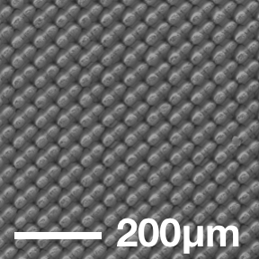
Ultrafast laser micromachining of surface modifications produce geometrical structures that conduct very precise functions. As the demand for device miniaturization continues, ultrafast or femtosecond laser micromachining produce surface reliefs on a micrometric or even nanometric scale and with high aspect ratios. Application examples Surface chevrons for enzyme reactions in point-of-care tests Lab-on-Chip microfluidic channels and microholes Security identification markings Creating diffractive, absorbent, adhesive surfaces 3D structuring of dielectrics, silicon, polymers, thin-films, integrated optics

2019-02-11T15:20:47+00:00May 14, 2018|
Go to Top