What we do
Laser micro-hole drilling
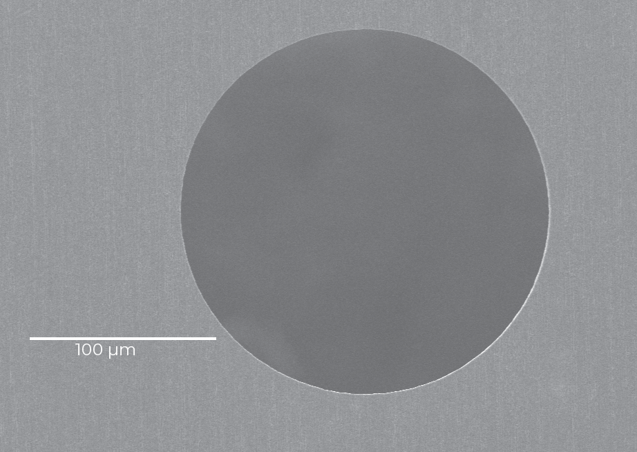
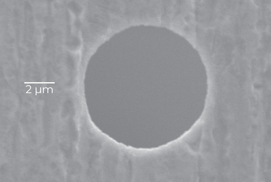
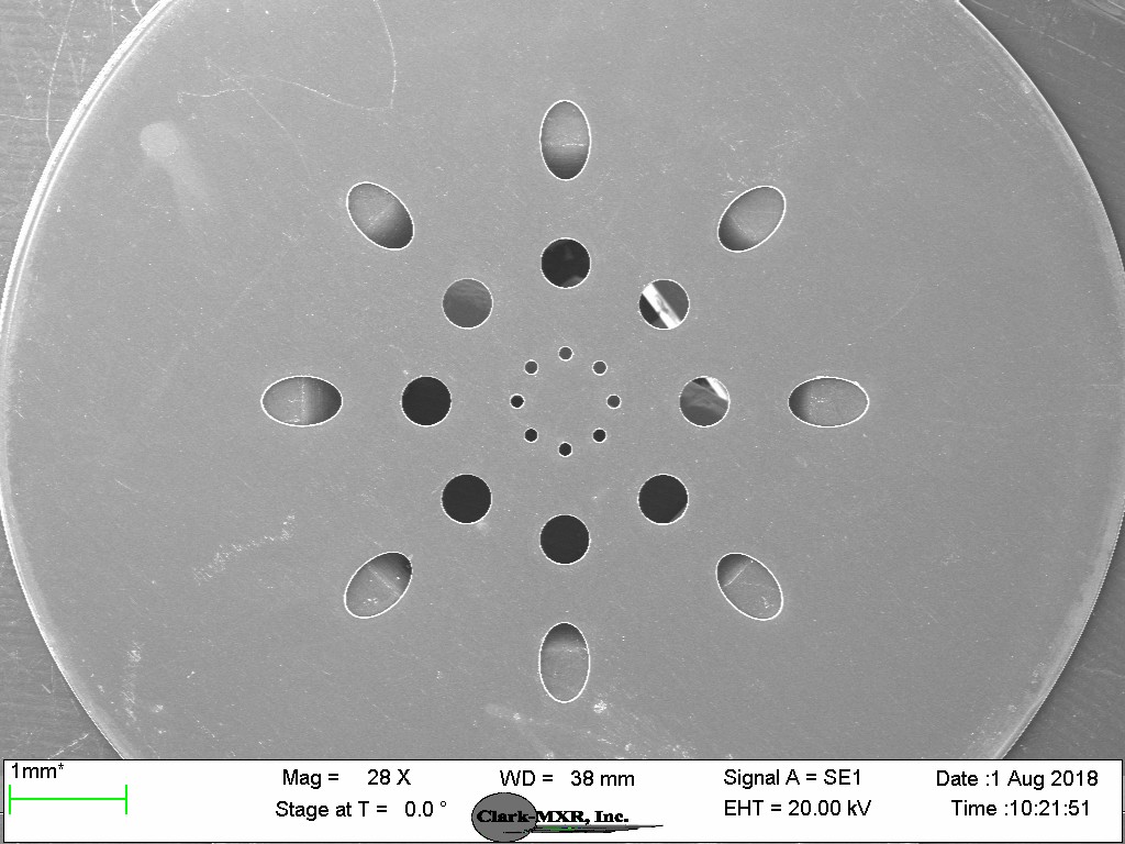
We drill holes from sub-micron to millimeter diameters, singly or in dense arrays, in metals, ceramics, glass and polymers. Typical work includes orifices and nozzles, filters, apertures, and arrays of closely spaced holes in thin foil or hardened tool steel where the wall between holes is only tens of microns. We control diameter, taper and position, and verify them on calibrated SEM and optical systems. Our standard diameter tolerance is within 5% of the hole diameter. Holes can be drilled to aspect ratios of up to 10:1 (depth to diameter). Standard apertures, pinholes and slits from 1 µm to 1 mm are listed on our Precision Apertures, Pinholes and Slits page.
Laser micro-cutting
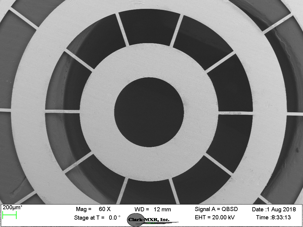
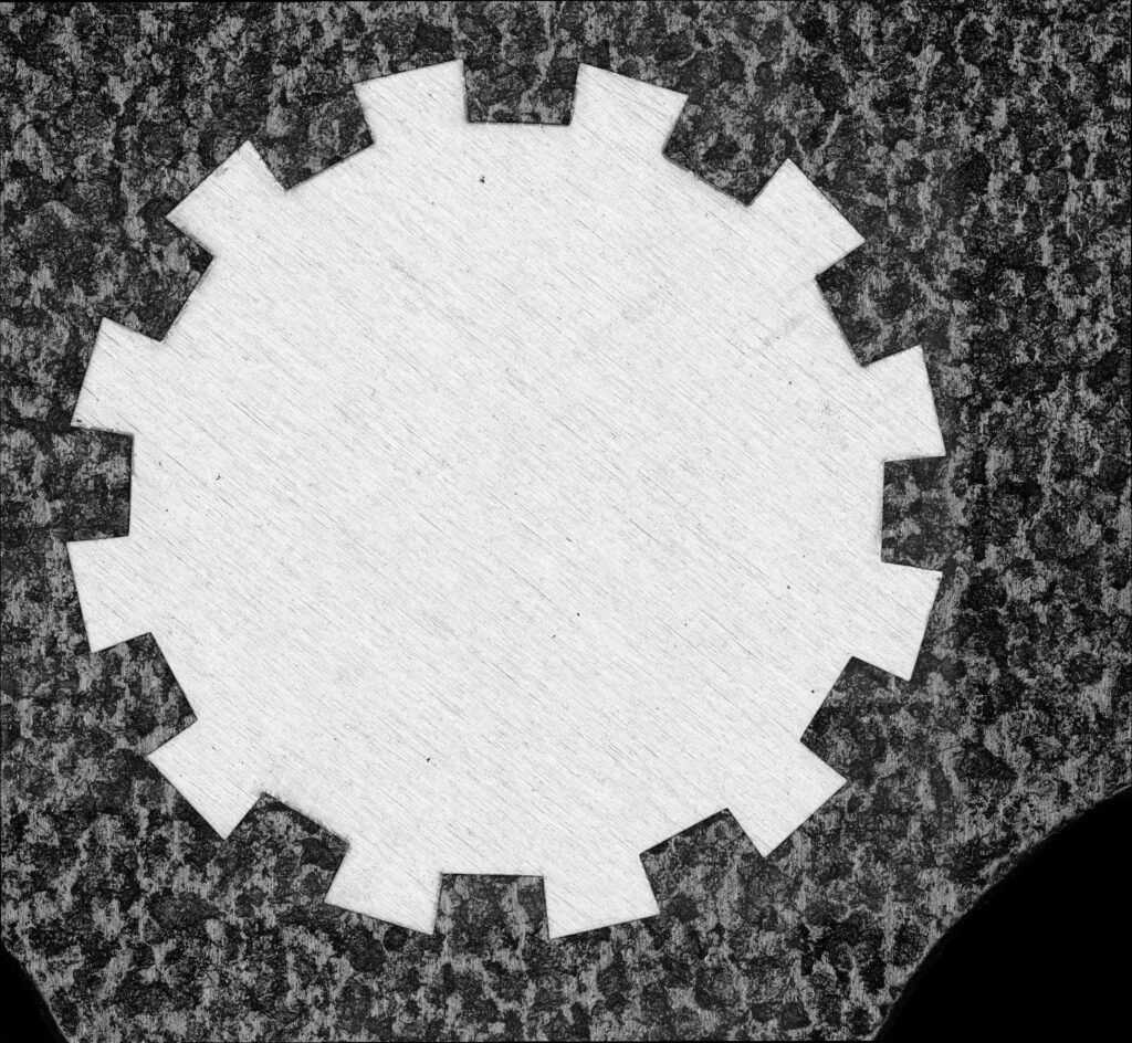
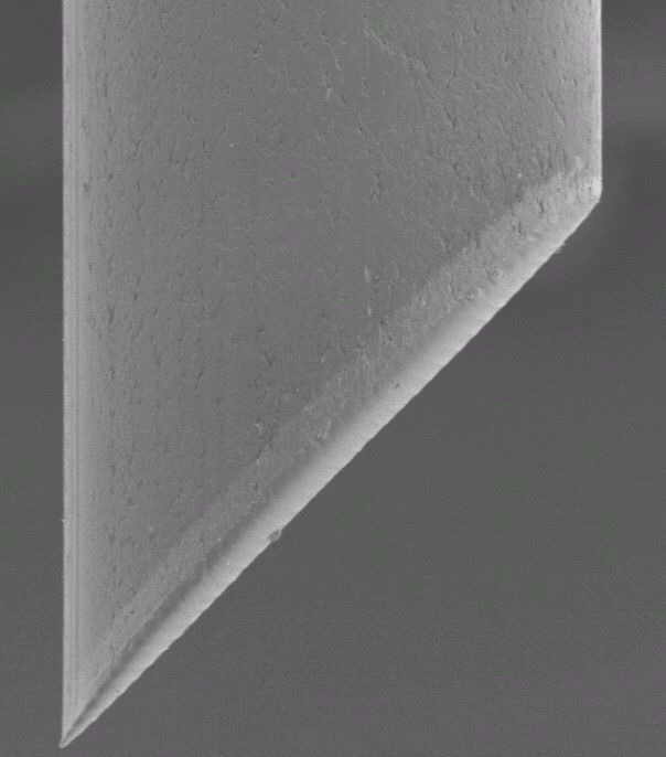
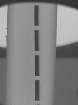
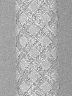
We cut fine features in foils, sheet, tubing and wafers, with kerf widths as narrow as 1 micron depending on material and thickness. Because the cut is athermal, thin and heat-sensitive parts stay flat and burr-free. Typical work includes cutting metal foils from 10 to 100 microns thick, apertures and slits, gears and springs, cut-outs in hypotubes and needles, and filaments in tungsten and other refractory metals. Where a cut-out leaves only narrow strips of material, internal stresses in the stock can make it move, so we review the design with you before quoting. We cut material up to 1 mm thick, and up to 3 mm for larger features.
Micromilling and controlled-depth machining
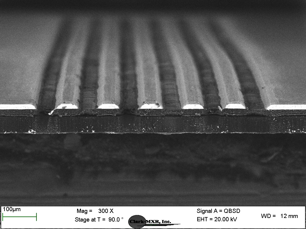
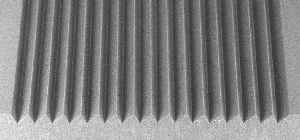
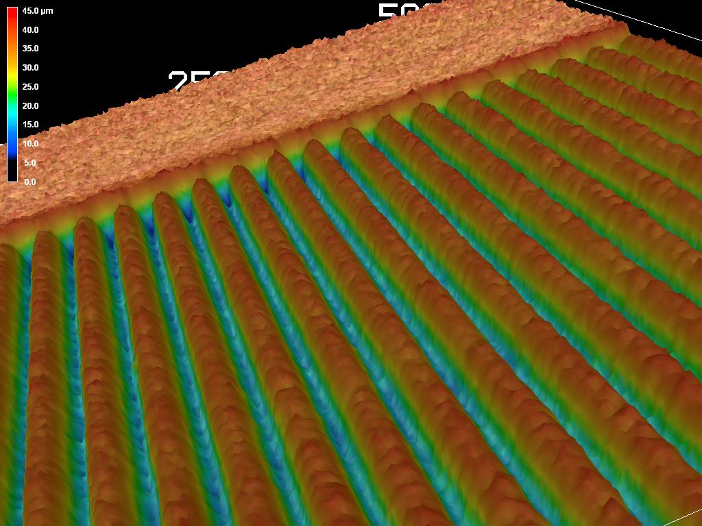
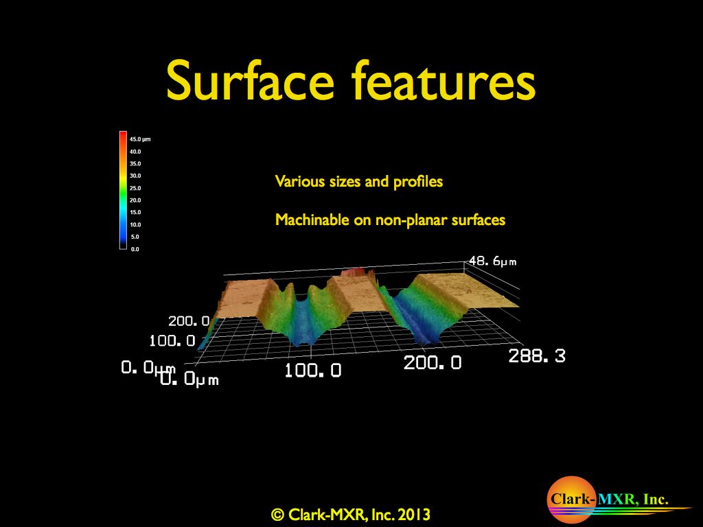
We remove material layer by layer to make blind pockets, channels, grooves, trenches and 3D surfaces, holding depth within a few percent of target. This includes thinning a selected area of foil to a set remaining thickness, and patterning a metal layer without damaging the polymer beneath it. Typical milled depths are up to 100 microns, with floor roughness around 5-10% of the depth.
Surface texturing and modification
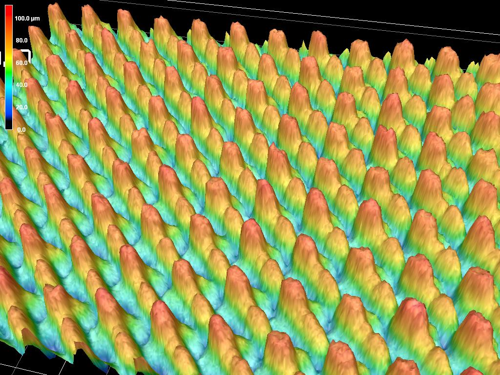
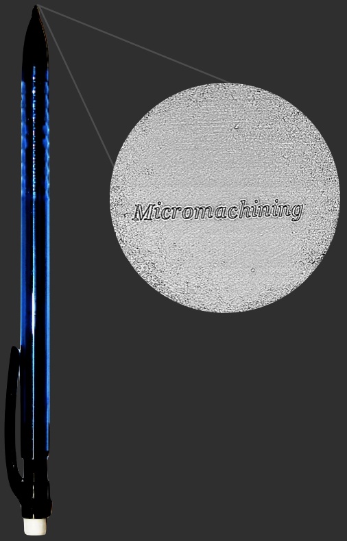
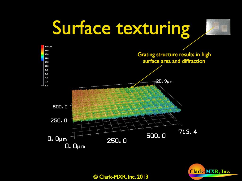
We create micro- and nano-scale textures and patterns on metals, ceramics, glass and polymers, controlling feature size, depth and placement to suit what your part needs to do: for example light-scattering and diffractive textures, anti-reflective surfaces, textures for adhesion and bonding, and drag or friction reduction. Textured areas can be placed precisely alongside untreated areas. Tell us the function you need from the surface and we will advise whether femtosecond texturing is a good fit.
Serial sectioning and sample preparation
We mill samples layer by layer for 3D tomography and failure analysis, exposing buried interfaces and microstructures without smearing or heat damage.
Inspection, cleaning and packaging
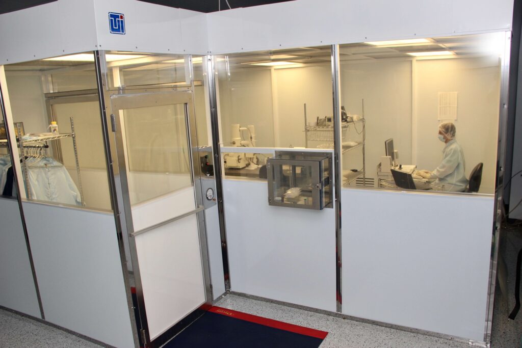
Every job can be measured and documented in-house using scanning electron microscopes, 3D laser confocal microscopy, vision measurement systems and CMM. Parts can be cleaned and shipped in cleanroom packaging up to ISO 5. Learn more about our inspection services.
Materials we machine
Femtosecond pulses work on almost any solid, including materials that are too hard, too brittle, too thin or too heat-sensitive for other methods.
| Material family | Examples |
|---|
| Metals and alloys | Stainless steel, hardened tool steel, titanium, nickel alloys such as Inconel, copper, aluminum, nitinol |
| Refractory and precious metals | Tungsten, tantalum, molybdenum, platinum, gold |
| Glass and crystals | Fused silica, borosilicate, sapphire, quartz, diamond |
| Ceramics | Zirconia, silicon carbide, silicon nitride, titanium nitride |
| Semiconductors | Silicon, germanium, gallium arsenide |
| Polymers | Polyimide, PEEK, PTFE, PMMA, biodegradable polymers |
| Thin films and layered materials | Metal on polymer, coatings, multilayer stacks |
Capabilities at a glance
| Capability | Value |
|---|
| Hole diameter | Sub-micron to millimeter scale (examples shown: 2 µm, under 10 µm, 0.2 mm) |
| Hole aspect ratio | Up to 10:1 (depth to diameter) |
| Kerf width | As narrow as 1 µm, depending on material and thickness |
| Blind-feature depth control | Within a few percent of target depth |
| Milling depth and finish | Typically up to 500 µm deep; floor roughness about 5-10% of depth |
| Dimensional tolerance | Depends on geometry and material. Drilled holes: diameter within 5% as standard. Cut-outs: material can shift as internal stresses release, especially where only narrow strips remain, so tolerances are agreed per part. |
| Maximum part size / travel | 300 × 300 × 25 mm |
| Material thickness range | Up to 1 mm (3 mm possible for larger features); contact us for thicker materials |
| Part geometry | Flat parts, and round parts (tubes, rods, wires) turned on a rotary axis, as on a lathe. Parts that need complex coordinated patterns, such as stents, are handled by our workstations for in-house use rather than as a service. |
| Quantities | Single prototypes to production runs in the thousands |
| Inspection | SEM, 3D laser confocal, optical, vision measurement, CMM |
| Packaging | Cleanroom packaging up to ISO 5 |
Industries we serve
- Semiconductor and electronics: apertures, probe and test components, thin-film patterning, and process development work tailored to a customer’s specific requirements.
- Medical devices and life sciences: cut and drilled tubing and needles, filters, microfluidic channels, and features in polymers and nitinol.
- Scientific instruments and research: apertures, pinholes and slits, tungsten filaments, optical scattering and calibration targets, sample preparation by serial sectioning. See precision components for instrument makers.
- Aerospace and automotive: flow-control orifices and nozzles, features in superalloys and ceramics.
How a project works
- Send us your requirement. A drawing or sketch, the material, the critical dimensions and the quantity. We sign NDAs on request.
- Feasibility review. Our engineers tell you whether we can make it, and suggest changes if a small design adjustment would improve the result.
- Samples or prototype. We machine first parts, often on your material, and send inspection data with them.
- Production. Once the process is proven, we run your quantity with the same documented process, inspection and packaging.
- Or bring it in-house. If volumes grow, the same process can transfer to a Clark-MXR workstation in your own facility. See our workstations.
Request a quote